Fermi Level In Semiconductors - With energy band diagram ,explain the variation of fermi ... - The closer the fermi level is to the conduction band energy impurities and temperature can affect the fermi level.
Fermi Level In Semiconductors - With energy band diagram ,explain the variation of fermi ... - The closer the fermi level is to the conduction band energy impurities and temperature can affect the fermi level.. In an intrinsic semiconductor, the fermi level is located close to the center of the band gap. Uniform electric field on uniform sample 2. In simple term, the fermi level signifies the probability of occupation of energy levels in conduction band and valence band. Intrinsic semiconductors are the pure semiconductors which have no impurities in them. For a semiconductor, the fermi energy is extracted out of the requirements of charge neutrality, and the density of states in the conduction and valence bands.
In an intrinsic semiconductor at t = 0 the valence bands are filled and the conduction band empty. The occupancy of semiconductor energy levels. Pentavalent impurities in a tetravalent semiconductor. Fermi level in an intrinsic semiconductor. Fermi level in extrinsic semiconductors.
Fermi level in extrinsic semiconductor from image.slidesharecdn.com Fermi level (ef) and vacuum level (evac) positions, work function (wf), energy gap (eg), ionization energy (ie), and electron affinity (ea) are parameters of great importance for any electronic material, be it a metal, semiconductor, insulator, organic, inorganic or hybrid. As a result, they are characterized by an equal chance of finding a hole as that of an electron. Fermi level is the term used to describe the top of the collection of electron energy levels at absolute zero temperature. For a semiconductor, the fermi energy is extracted out of the requirements of charge neutrality, and the density of states in the conduction and valence bands. P = n = ni. Similar questions asked by users. Fermi level is the energy that corresponds to the center of gravity of the conduction electrons and holes weighted according to their energies. Fermi level in the middle of forbidden band indicates equal concentration of free electrons and holes.
Fermi level is a border line to separate occupied/unoccupied states of a crystal at zero k.
Fermi level in extrinsic semiconductors. P = n = ni. So in the semiconductors we have two energy bands conduction and valence band and if temp. Fermi level in the middle of forbidden band indicates equal concentration of free electrons and holes. Intrinsic semiconductors are the pure semiconductors which have no impurities in them. Fermi level in an intrinsic semiconductor. Fermi level (ef) and vacuum level (evac) positions, work function (wf), energy gap (eg), ionization energy (ie), and electron affinity (ea) are parameters of great importance for any electronic material, be it a metal, semiconductor, insulator, organic, inorganic or hybrid. If you found this article informative then please share it with your friends. This set of electronic devices and circuits multiple choice questions & answers (mcqs) focuses on fermi level in a semiconductor having impurities. The fifth electron of donor atom is loosely bounded. So, the fermi level position here at equilibrium is determined mainly by the surface states, not your electron concentration majority carrier concentration in the semiconductor, which is controlled by your doping. Pentavalent impurities in a tetravalent semiconductor. What is fermi energy level in semiconductors?
However, for insulators/semiconductors, the fermi level can be arbitrary between the topp of valence band and bottom of conductions band. Fermi level is the energy that corresponds to the center of gravity of the conduction electrons and holes weighted according to their energies. The fifth electron of donor atom is loosely bounded. I hope you get the idea about what is fermi energy level in semiconductors. In all cases, the position was essentially independent of the metal.
GATE 1989 Effect on Fermi level position of extrinsic ... from i.ytimg.com Similar questions asked by users. We mentioned earlier that the fermi level lies within the forbidden gap, which basically results from the need to maintain equal concentrations of electrons and (15) and (16) be equal at all temperatures, which yields the following expression for the position of the fermi level in an intrinsic semiconductor Fermi level is the energy that corresponds to the center of gravity of the conduction electrons and holes weighted according to their energies. 5 fermi level and variation of fermi level with temperature in an intrinsic semiconductor. Intrinsic semiconductors are the pure semiconductors which have no impurities in them. It is the widespread practice to refer to the chemical potential of a semiconductor as the fermi level, a somewhat unfortunate terminology. Fermi level in the middle of forbidden band indicates equal concentration of free electrons and holes. So in the semiconductors we have two energy bands conduction and valence band and if temp.
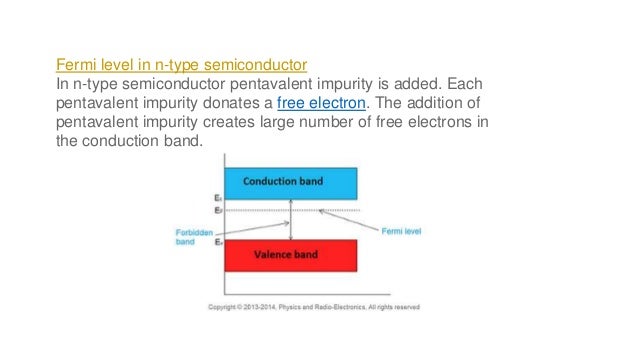
Each pentavalent impurity donates a free electron.
It is well estblished for metallic systems. The fermi level determines the probability of electron occupancy at different energy levels. Charge carrier densities and fermi level in extrinsic semiconductors strongly depend on temperature and impurity density. I hope you get the idea about what is fermi energy level in semiconductors. Fermi level is the term used to describe the top of the collection of electron energy levels at absolute zero temperature. Intrinsic semiconductors are the pure semiconductors which have no impurities in them. The fermi level does not include the work required to remove the electron from wherever it came from. 5 fermi level and variation of fermi level with temperature in an intrinsic semiconductor. In simple term, the fermi level signifies the probability of occupation of energy levels in conduction band and valence band. In all cases, the position was essentially independent of the metal. The occupancy of semiconductor energy levels. 10 we can deduce that the fermi level e f must be in the middle of the bandgap for an intrinsic semiconductor, as seen in figure 4. It can be written as.
It is a thermodynamic quantity usually denoted by µ or ef for brevity. However, it is rather difficult to tune φ for 2d mx2 by using different common metals because of the effect of fermi level pinning (flp). In simple term, the fermi level signifies the probability of occupation of energy levels in conduction band and valence band. P = n = ni. 10 we can deduce that the fermi level e f must be in the middle of the bandgap for an intrinsic semiconductor, as seen in figure 4.
Fermi level in extrinsic semiconductor from image.slidesharecdn.com 10 we can deduce that the fermi level e f must be in the middle of the bandgap for an intrinsic semiconductor, as seen in figure 4. Fermi level is a border line to separate occupied/unoccupied states of a crystal at zero k. Increases the fermi level should increase, is that. Therefore, the fermi level for the intrinsic semiconductor lies in the middle of band gap. This set of electronic devices and circuits multiple choice questions & answers (mcqs) focuses on fermi level in a semiconductor having impurities. The fifth electron of donor atom is loosely bounded. It can be written as. Pentavalent impurities in a tetravalent semiconductor.
Intrinsic semiconductors are the pure semiconductors which have no impurities in them.
Charge carrier densities and fermi level in extrinsic semiconductors strongly depend on temperature and impurity density. Each pentavalent impurity donates a free electron. Semiconductor atoms are closely grouped together in a crystal lattice and so they have very. The fermi level does not include the work required to remove the electron from wherever it came from. The fermi level determines the probability of electron occupancy at different energy levels. P = n = ni. Fermi level is the term used to describe the top of the collection of electron energy levels at absolute zero temperature. Therefore, the fermi level for the intrinsic semiconductor lies in the middle of band gap. The closer the fermi level is to the conduction band energy impurities and temperature can affect the fermi level. However, it is rather difficult to tune φ for 2d mx2 by using different common metals because of the effect of fermi level pinning (flp). • the fermi function and the fermi level. The occupancy of semiconductor energy levels. 5 fermi level and variation of fermi level with temperature in an intrinsic semiconductor.
Fermi level is the term used to describe the top of the collection of electron energy levels at absolute zero temperature fermi level in semiconductor. Charge carrier densities and fermi level in extrinsic semiconductors strongly depend on temperature and impurity density.


0 Komentar